

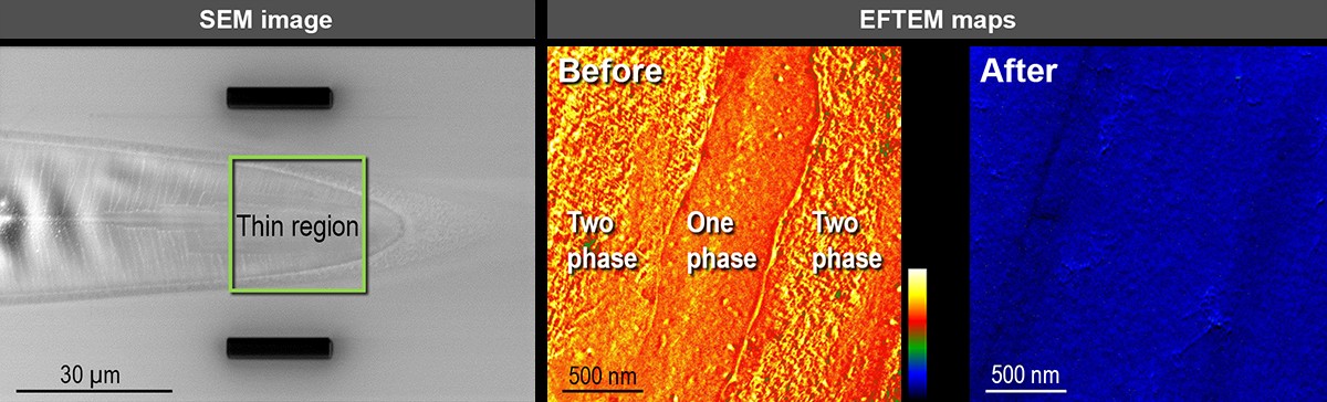
Achieving atomic-resolution microscopy of Al-Cu thin films on electron-transparent silicon nitride TEM grids is hindered by the limitations of conventional preparation techniques. Dimpling, grinding, and standard ion milling are incompatible with the grid's fragile and stressed silicon nitride window. Additionally, the focused ion beam (FIB) lift-out technique risks rupturing the stressed windows, which can cause specimen loss. Ga contamination during FIB milling poses a further challenge, potentially causing room-temperature diffusion and liquid metal embrittlement [1] on the Al-Cu thin film. Consequently, concentrated Ar ion beam milling is presented as a viable site-specific method for plan-view atomic-resolution analysis of Al-Cu thin films on silicon nitride grids.
Fiducial markers (SEM image) were created using electron beam-assisted Pt deposition within a FIB system. Subsequent thinning of the sample was performed using low-energy, concentrated Ar ion beam milling using Fischione Instruments’ Model 1040 NanoMill® TEM specimen preparation system. This procedure yielded a TEM specimen with a large field of view, approximately 1000 μm², with minimal damage to the surrounding material. The resulting thin sections, characterized by EFTEM, enabled atomic-resolution imaging of θ’‑Al2Cu precipitates formed via aging by solid-state phase transformation in Al-Cu alloys [2]. This methodology is applicable to specimens on silicon nitride TEM grids following in situ TEM studies, enabling subsequent atomic-resolution imaging.
[1] Stumpf, R., & Feibelman, P. J. (1996). Towards an understanding of liquid-metal embrittlement: Energetics of Ga on Al surfaces. Physical Review. B, Condensed Matter, 54(7), 5145–5150.
[2] Vishwanadh, B., Jo, J., Bonifacio, C. S., & Wiezorek, J. M. (2022). Site-specific preparation of plan-view samples with a large field of view for atomic resolution STEM and TEM studies of rapidly solidified multi-phase Al Cu thin films. Materials Characterization, 189, 111943.
Learn more
- Bonifacio, C., Vishwanadh, B., Jo, J., Ray, M., Wiezorek, J., & Fischione, P. (2022). Site-specific sample preparation by concentrated Ar ion milling for post-mortem atomic resolution imaging of rapidly solidified AL-CU thin films after pulsed laser melting. Microscopy and Microanalysis, 28(S1), 124–125.
- Chung, T., Yang, Y., Hsiao, C., Li, W., Huang, B., Tsao, C., Shi, Z., Lin, J., Fischione, P. E., Ohmura, T., & Yang, J. (2018). Morphological evolution of GP zones and nanometer-sized precipitates in the AA2050 aluminium alloy.International Journal of Lightweight Materials and Manufacture, 1(3), 142–156.
Contact us on 01582 764334 to speak with one of our Product Specialists.
Lambda Photometrics is the leading UK Distributor of Characterisation, Measurement and Analysis solutions with particular expertise in Instrumentation, Laser & Light based products, Optics, Electro-optic Testing, Spectroscopy, Machine Vision, Optical Metrology, Fibre Optics, Microscopy and Anti-vibration tables & custom solutions
-
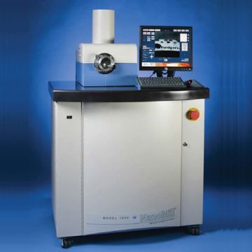
Fischione Model 1040 NanoMill® TEM Specimen Preparation System
- Ultra-low energy ion source
- Concentrated ion beam
- Removes amorphous and implanted layers
- Ideal for post-focused ion beam processing and milling of conventionally prepared specimens
- Liquid nitrogen-cooled specimen stage