Tue, May 25, 2021 3:00 PM - 4:00 PM BST
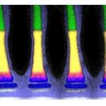
Transmission electron microscopy (TEM) is a critical characterization tool for the semiconductor industry. Gallium focused ion beam (FIB) is frequently used for TEM specimen preparation; however, FIB milling typically results in specimen artifacts, such as surface amorphisation and gallium-implanted layers, both of which may limit analytical and high-resolution electron microscopy. In this webinar, we will present concentrated argon ion beam milling as a post-FIB polishing step for precise and reproducible specimen preparation of advanced semiconductor devices. We will show in situ and ex situ FIB-prepared TEM specimens that are free from FIB artifacts (Ga implantation and curtaining) and have a thicknesses of less than 20 nm after concentrated ion beam milling. High throughput workflow will also be described.


