

Precise, reliable, characterisation of thin film topography and thickness, and substrate topography.
 Thin transparent thin films are critical across a variety of markets and applications, including consumer electronics, semiconductors and optics. Precise monitoring and control of thin film processes is achieved by measuring top surface, thickness, and substrate surface characteristics – all of which are enabled by multiple thin film measurement and analysis technologies available on ZYGO's 3D optical profilers.
In an ideal world, a surface metrology technology developed to measure submicron films will retain its performance for topography alone. This takes account of metrics, such as resolution and throughput and even the configuration flexibility. For microscope based technologies, this means that films analysis should not restrict the choice of objective or zoom.
For thick films, the signals are well separated and can be easily distinguished between the top surface and the substrate. However, a transparent film will generally produce an additional signal from the substrate and therefore the surface and substrate signals merge and are no longer separable. But this sensitivity to films also gives the opportunity for the distorted CSI signal to be decoded to simultaneously determine surface and thickness.

Fig1. Typical CSI signals for (a) bare surface (no film); (b) thick film (well over 1µm) with well-separated signals from surface to substrate; and (c) submicron film with merged surface and substrate signals.
Advanced Model Based Analysis (MBA) is the most advanced CSI-based thin film measurement technique available from ZYGO, and works by comparing a theoretical model of the sample film stack to an actual measurement signal as seen by the profiler. This patented technology simultaneously measures topography, thickness, and substrate topography for single layer films from 50–2000nm in seconds. In addition to thin film characterisation, MBA technology can be used to perform true topography measurements of dissimilar materials by adjusting for the phase change on reflection (PCOR) that occurs in these situations.
Standard Film Analysis (LSQ) is used to measure film thickness and substrates of films from 1–150µm optical thickness, as well as the top surface of films from 0.4–150µm. Thick film metrology works by isolating the interference signals that are created by the multiple material interfaces and require only basic knowledge of the film's index of refraction.
Because they are based on CSI technology, there are several advantages that MBA and LSQ thin film measurement technologies provide compared to other techniques:
- 3D areal surface maps provide context for understanding a process that cannot be observed when film metrology is reduced to a single thickness number.
- Film measurement is performed through-the-lens, which helps to ensure that the region of interest is exactly the region profiled.
- No additional hardware is required for most applications of MBA or LSQ thin film measurement.
Standard Film Analysis (LSQ) is available as an option on NewView 9000, Nexview and Nexview NX2 profilers, while Advanced Model Based Analysis (MBA) is available as an option exclusively on the Nexview and Nexview NX2 platforms.
To speak with a Sales & Applications Engineer please call 01582 764334 or click here to email.
Lambda Photometrics is a leading UK Distributor of Characterisation, Measurement and Analysis solutions with particular expertise in Electronic/Scientific and Analytical Instrumentation, Laser and Light based products, Optics, Electro-optic Testing, Spectroscopy, Machine Vision, Optical Metrology, Fibre Optics and Microscopy.
-
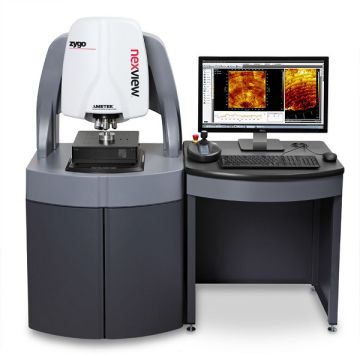
Zygo Nexview™
The Nexview has been superseded by the Nexview NX2. We have a 2018 ex-demonstration Nexview system for sale. Please contact us for more information.
Nexview 3D optical surface profiler excels at measuring all surfaces – from super-smooth to very rough, with sub-nanometer precision, independent of field of view.
-

Zygo Nexview™ NX2
For ultra performance and industry-leading speed, precision, and automation. Designed for the most demanding applications. Measure virtually any surface! -

Zygo NewView™ 9000
High performance optical profiler. Well suited for a wide range of applications, and highly configurable to meet your needs!